
Design
Design & Layout
• The DLA Emulation Programs utilize current Electronic Design Automation (EDA) tools
• Process Design Kits (PDKs) are updated as new processes, technologies, and
capabilities become available
• Controlled Unclassified Information (CUI) and Cybersecurity Maturity Model
Certification (CMMC) compliant network cluster of workstations and servers
used to support high uptime and availability of EDA software and data
• Data is backed up regularly and off-site storage is used to guard against data loss
Design
- Netlist development and simulation
Schematic capture
SPICE simulation
Behavioral simulation
Synthesis
Static timing analysis
Cell characterization
Fault coverage vector generation
Fault coverage analysis
Design-for-test (DFT)
Formal Equivalence Check

Layout
- Place and route
- Layout capture
- Layout verification LVS/DRC/ERC
- DRC Deck Generation
- Interconnect parasitic extraction
- IR/Thermal/Power/EM Analysis
• Experienced in Digital and Analog IC design across all the semiconductor processes supported by the co-located Microcircuit Emulation Center’s Wafer Foundry
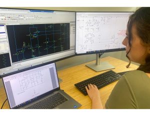
• MEC designers work closely with our on-site Trusted foundry and use advanced TCAD tools to simulate the fabrication process, and along with physical device modeling provides the Emulation Programs with the unique capability to meet customers’ requirements and provide microcircuits that are in full conformance with customer specifications
• Design libraries for each process are characterized over the full military temperature and voltage ranges
• Design flow can handle the synthesis and place & route of any combination of in-house and externally generated Hardware Description Language (HDL) Intellectual Property (IP) Cores onto our gate array processes
• Layout of designs are performed using place & route tools 
• Characterization of parasitic capacitance and resistance of the back-end-of-line (BEOL) process creates back-annotated netlists to verify microcircuit performance to required specification when manufactured
• Digital and analog design capability covers a range of technologies (CMOS, BiCMOS, Bipolar), complexity and feature sizes, over 3.0 μm down to 0.35 μm
• Current development thrust is to add capability to emulate analog microcircuits to support warfighter needs.