Base Wafers and Gate Arrays
Base Wafers and Gate Arrays
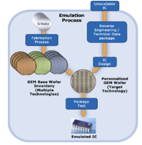
The Emulation programs have developed a split manufacturing process, in which wafer lots are processed through the majority of the manufacturing flow and held in inventory. This technology is based on gate arrays fabricated with predefined circuit elements (base wafers) which are interconnected by multiple levels of metal conductors (wafer personalization) and minimizes the wafer production time for emulated devices. This approach allows Integrated Circuits (ICs) that were originally manufactured in diverse technologies to be produced from a managed inventory of standardized base wafers. An overview of the GEM Production System for emulating microcircuits is illustrated below.
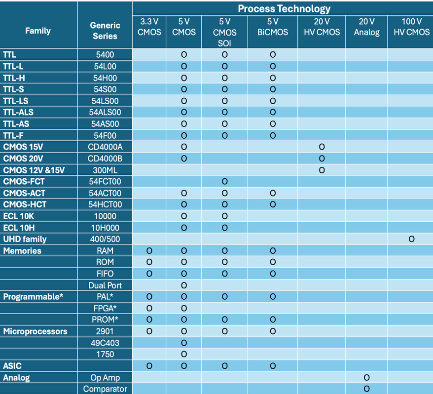
The technologies offered by the Emulation Programs have been expanded over time. The initial focus was TTL (Transistor Transistor Logic) 5-Volt logic families and ECL (Emitter Coupled Logic) devices. Over time new arrays were developed to emulate higher speed and lower power variations of these families. Technologies were also developed to emulate CMOS logic devices with power supplies up to 20-Volts. Smaller node sizes were implemented to emulate more complex ASIC and programmable logic arrays and memory devices. The current technologies can support emulations of user or field programmable devices. Programmable logic or memory devices are emulated using the metal personalization mask during the wafer fabrication. The devices are permanently programmed and verified to be the functional equivalent of the original programmed device.
The table below highlights the current Emulation technologies by process technology, and applications.


